ADC0804 Pin-out and Typical Connections
As shown in the typical circuit, ADC0804 can be interfaced with any microcontroller. You need a minimum of 11 pins to interface ADC0804, eight for data pins and 3 for control pins. As shown in the typical circuit the chip select pin can be made low if you are not using the microcontroller port for any other peripheral (multiplexing).
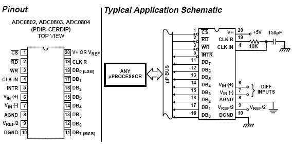
ADC0804 Pin Diagram
There is a universal rule to find out how to use an IC. All you need is the datasheet of the IC you are working with and take a look at the timing diagram of the IC which shows how to send the data, which signal to assert and at what time the signal should be made high or low etc.
Note: Keep this in mind that whenever you are working with an IC and you want to know how to communicate with that IC, then simply look into the timing diagram of that IC from its datasheet. It gives you complete information that you need regarding the communication of IC.
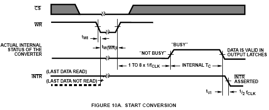
Start Conversion Timing Diagram
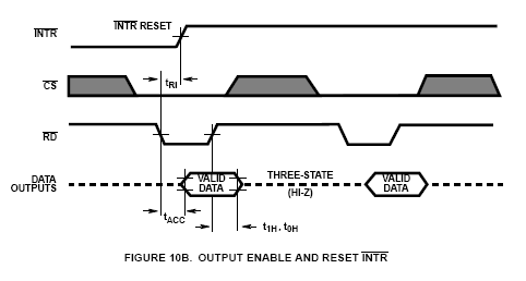
End of Conversion Timing Diagram
The above timing diagrams are from ADC0804 datasheet. The first diagram (FIGURE 10A) shows how to start a conversion. Also you can see which signals are to be asserted and at what time to start a conversion. So looking into the timing diagram FIGURE 10A. We note down the steps or say the order in which signals are to be asserted to start a conversion of ADC. As we have decided to make Chip select pin as low so we need not to bother about the CS signal in the timing diagram. Below steps are for starting an ADC conversion. I am also including CS signal to give you a clear picture. While programming we will not use this signal.
- Make chip select (CS) signal low.
- Make write (WR) signal low.
- Make chip select (CS) high.
- Wait for INTR pin to go low (means conversion ends).
Once the conversion in ADC is done, the data is available in the output latch of the ADC. Looking at the FIGURE 10B which shows the timing diagram of how to read the converted value from the output latch of the ADC. Data of the new conversion is only avalable for reading after ADC0804 made INTR pin low or say when the conversion is over. Below are the stepts to read output from the ADC0804.
- Make chip select (CS) pin low.
- Make read (RD) signal low.
- Read the data from port where ADC is connected.
- Make read (RD) signal high.
- Make chip select (CS) high.
- rd equ P1.0 ;Read signal P1.0
- wr equ P1.1 ;Write signal P1.1
- cs equ P1.2 ;Chip Select P1.2
- intr equ P1.3 ;INTR signal P1.3
- adc_port equ P2 ;ADC data pins P2
- adc_val equ 30H ;ADC read value stored here
- org 0H
- start: ;Start of Program
- acall conv ;Start ADC conversion
- acall read ;Read converted value
- mov P3,adc_val ;Move the value to Port 3
- sjmp start ;Do it again
- conv: ;Start of Conversion
- clr cs ;Make CS low
- clr wr ;Make WR Low
- nop
- setb wr ;Make WR High
- setb cs ;Make CS high
- wait:
- jb intr,wait ;Wait for INTR signal
- ret ;Conversion done
- read: ;Read ADC value
- clr cs ;Make CS Low
- clr rd ;Make RD Low
- mov a,adc_port ;Read the converted value
- mov adc_val,a ;Store it in local variable
- setb rd ;Make RD High
- setb cs ;Make CS High
- ret ;Reading done
8051 C program for ADC0804
- #include <REGX51.H>
- #define adc_port P2 //ADC Port
- #define rd P1_0 //Read signal P1.0
- #define wr P1_1 //Write signal P1.1
- #define cs P1_2 //Chip Select P1.2
- #define intr P1_3 //INTR signal P1.3
- void conv(); //Start of conversion function
- void read(); //Read ADC function
- unsigned char adc_val;
- void main() {
- while (1) { //Forever loop
- conv(); //Start conversion
- read(); //Read ADC
- P3 = adc_val; //Send the read value to P3
- }
- }
- void conv() {
- cs = 0; //Make CS low
- wr = 0; //Make WR low
- wr = 1; //Make WR high
- cs = 1; //Make CS high
- while (intr); //Wait for INTR to go low
- }
- void read() {
- cs = 0; //Make CS low
- rd = 0; //Make RD low
- adc_val = adc_port; //Read ADC port
- rd = 1; //Make RD high
- cs = 1; //Make CS high
- }